- 您现在的位置:买卖IC网 > Sheet目录3842 > PIC18LF6390-I/PT (Microchip Technology)IC PIC MCU FLASH 4KX16 64TQFP
RL78/G13
CHAPTER 4 PORT FUNCTIONS
R01UH0146EJ0100 Rev.1.00
186
Sep 22, 2011
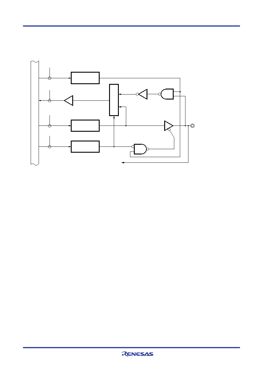
For example, figure 4-15 shows a block diagram of port 2 for 128-pin products when PIOR = 00H.
Figure 4-15. Block Diagram of P20 to P27
P20/ANI0/AVREFP,
P21/ANI1/AVREFM,
P22/ANI2 to P27/ANI7
RD
WRPORT
WRPM
PM20 to PM27
PM2
A/D converter
P2
Output latch
(P20 to P27)
Selector
Internal
bus
WRADPC
ADPC3 to ADPC0
ADPC
0:Analog input
1:Digital I/O
ADPC:
A/D port configuration register
P2:
Port register 2
PM2:
Port mode register 2
RD:
Read signal
WR
××: Write signal
<R>
发布紧急采购,3分钟左右您将得到回复。
相关PDF资料
DSPIC30F3013-30I/SP
IC DSPIC MCU/DSP 24K 28DIP
DSPIC33FJ32MC202-E/SO
IC DSPIC MCU/DSP 32K 28SOIC
52745-0896
CONN FFC 8POS .5MM R/A ZIF SMD
52745-0496
CONN FFC 4POS .5MM R/A ZIF SMD
TS87C58X2-LCE
IC MCU 8BIT 32K OTP 30MHZ 44VQFP
TS87C54X2-VCE
IC MCU 8BIT 16K OTP 40MHZ 44VQFP
TS87C54X2-VIE
IC MCU 8BIT 16K OTP 40MHZ 44VQFP
52746-1670
CONN FFC 16POS .5MM R/A ZIF SMD
相关代理商/技术参数
PIC18LF6390T-I/PT
功能描述:8位微控制器 -MCU 8 KB FL 768 RoHS:否 制造商:Silicon Labs 核心:8051 处理器系列:C8051F39x 数据总线宽度:8 bit 最大时钟频率:50 MHz 程序存储器大小:16 KB 数据 RAM 大小:1 KB 片上 ADC:Yes 工作电源电压:1.8 V to 3.6 V 工作温度范围:- 40 C to + 105 C 封装 / 箱体:QFN-20 安装风格:SMD/SMT
PIC18LF6393-I/PT
功能描述:8位微控制器 -MCU 128 Segmnt LCD DRVR 12B ADC 8KB 768BRAM RoHS:否 制造商:Silicon Labs 核心:8051 处理器系列:C8051F39x 数据总线宽度:8 bit 最大时钟频率:50 MHz 程序存储器大小:16 KB 数据 RAM 大小:1 KB 片上 ADC:Yes 工作电源电压:1.8 V to 3.6 V 工作温度范围:- 40 C to + 105 C 封装 / 箱体:QFN-20 安装风格:SMD/SMT
PIC18LF6393T-I/PT
功能描述:8位微控制器 -MCU 128 Segmnt LCD DRVR 12B ADC 8KB 768BRAM RoHS:否 制造商:Silicon Labs 核心:8051 处理器系列:C8051F39x 数据总线宽度:8 bit 最大时钟频率:50 MHz 程序存储器大小:16 KB 数据 RAM 大小:1 KB 片上 ADC:Yes 工作电源电压:1.8 V to 3.6 V 工作温度范围:- 40 C to + 105 C 封装 / 箱体:QFN-20 安装风格:SMD/SMT
PIC18LF6410-I/PT
功能描述:8位微控制器 -MCU 16kBF 768RM 68 I/O RoHS:否 制造商:Silicon Labs 核心:8051 处理器系列:C8051F39x 数据总线宽度:8 bit 最大时钟频率:50 MHz 程序存储器大小:16 KB 数据 RAM 大小:1 KB 片上 ADC:Yes 工作电源电压:1.8 V to 3.6 V 工作温度范围:- 40 C to + 105 C 封装 / 箱体:QFN-20 安装风格:SMD/SMT
PIC18LF6410T-I/PT
功能描述:8位微控制器 -MCU 16 KB FL 768 RAM 68 I/O RoHS:否 制造商:Silicon Labs 核心:8051 处理器系列:C8051F39x 数据总线宽度:8 bit 最大时钟频率:50 MHz 程序存储器大小:16 KB 数据 RAM 大小:1 KB 片上 ADC:Yes 工作电源电压:1.8 V to 3.6 V 工作温度范围:- 40 C to + 105 C 封装 / 箱体:QFN-20 安装风格:SMD/SMT
PIC18LF6490-I/PT
功能描述:8位微控制器 -MCU 16kBF 768RM 68 I/O RoHS:否 制造商:Silicon Labs 核心:8051 处理器系列:C8051F39x 数据总线宽度:8 bit 最大时钟频率:50 MHz 程序存储器大小:16 KB 数据 RAM 大小:1 KB 片上 ADC:Yes 工作电源电压:1.8 V to 3.6 V 工作温度范围:- 40 C to + 105 C 封装 / 箱体:QFN-20 安装风格:SMD/SMT
PIC18LF6490T-I/PT
功能描述:8位微控制器 -MCU 16 KB FL 768 RAM 68 I/O RoHS:否 制造商:Silicon Labs 核心:8051 处理器系列:C8051F39x 数据总线宽度:8 bit 最大时钟频率:50 MHz 程序存储器大小:16 KB 数据 RAM 大小:1 KB 片上 ADC:Yes 工作电源电压:1.8 V to 3.6 V 工作温度范围:- 40 C to + 105 C 封装 / 箱体:QFN-20 安装风格:SMD/SMT
PIC18LF6493-I/PT
功能描述:8位微控制器 -MCU 128 Segmnt LCD DRVR 12B ADC 16KB 768BRAM RoHS:否 制造商:Silicon Labs 核心:8051 处理器系列:C8051F39x 数据总线宽度:8 bit 最大时钟频率:50 MHz 程序存储器大小:16 KB 数据 RAM 大小:1 KB 片上 ADC:Yes 工作电源电压:1.8 V to 3.6 V 工作温度范围:- 40 C to + 105 C 封装 / 箱体:QFN-20 安装风格:SMD/SMT